PCB Designs
Overview
This portfolio showcases my previous work in PCB design and fabrication. It includes pictures of various PCBs that I have designed or fabricated. The last 2 years I have done designs with Eagle, KiCAD and Altium.
I am a junior electronic engineer with experience in designing and fabricating PCBs. On my own, I have designed 8 PCBs, including microcontroller based boards, development boards, and power supplies.
My skills in PCB design and fabrication include:
- Designing and routing PCBs using Eagle CAD
- Knowledge of PCB layout design principles
- Creating custom footprints for components
- Generating Gerber and Excellon files for fabrication
- Selecting appropriate components and connectors for specific applications
- Soldering and assembling PCBs
- Familiarity with various fabrication techniques such as SMT and through-hole assembly
Designs
This portfolio includes pictures of the following PCBs that I have designed and fabricated in my free time. Some designs have IP because I designed when I was working with a company related, so they are not here :c.
| Dev board design for ad-hoc data acquisition of resistive sensors | ||
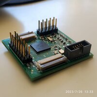 | ||
| Layers | Dimensions | Software |
|---|---|---|
| 4 | 30x10 [cm] | Eagle |
| Designed | Fabricated | Tested |
| 2023-07-26 | ✅ | ✅ |
| SCHEMATIC GERBER | ||
| A practice PCB for learning KiCAD. | ||
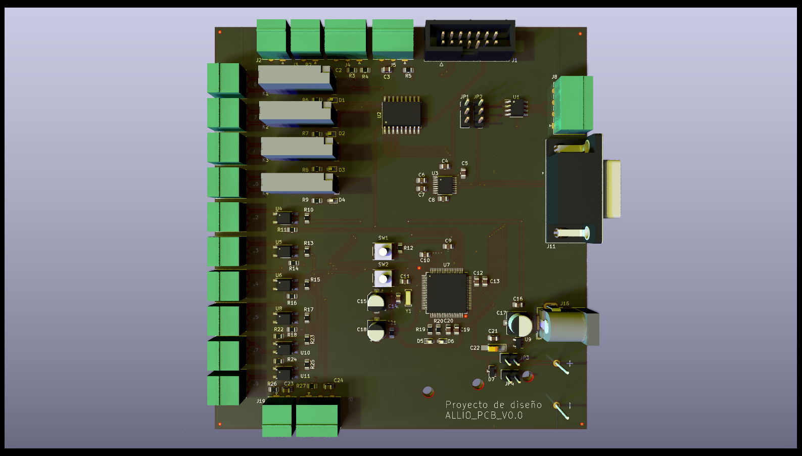 | ||
| PCB designed in the university master's program. | ||
| Layers | Dimensions | Software |
|---|---|---|
| 2 | 11.2x12.1 [cm] | KiCAD |
| Designed | Fabricated | Tested |
| 2025-05-07 | ❌ | ❌ |
| SCHEMATIC GERBER | ||
| Practice PCB for learning KiCAD. | ||
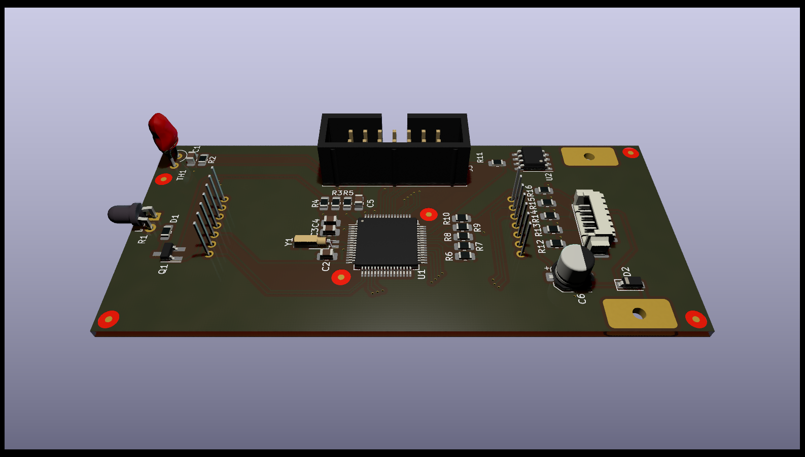 | ||
| PCB designed in the university master's program. | ||
| Layers | Dimensions | Software |
|---|---|---|
| 2 | 9x4 [cm] | KiCAD |
| Designed | Fabricated | Tested |
| 2023-05-14 | ❌ | ❌ |
| SCHEMATIC GERBER | ||
Useful Software for PCB design
Contact
If you are interested in my services for your next PCB design and fabrication project, please feel free to contact me.
Email: